Intro
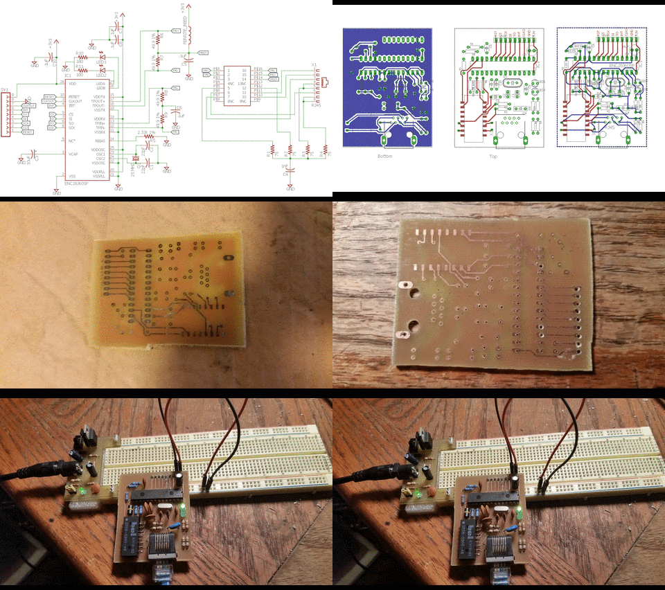
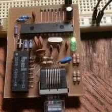 Make everything an internet of things, don’t worry about the ‘s’. IOT devices are very common and wireless with esp8266 and Arduino sketch will have you blinking an internet connected LED in no time, but what about a low speed, wired option with a large footprint - said no one ever. ENC28J60 breakout boards can have a small footprint with surface mount components, mag jack and ssop or soic package size ENC28J60 component. I decided to make use of an PDIP ENC28J60 chip I had laying around and salvaged components from a broken NIC, so this is a larger footprint. This PCB project is double sided with traces on top and bottom. If the layers aren’t matched up just right, the drill holes might not meet up with the pads, and it could be a problem. Here’s how I made sure both sides of the pcb matched up: dual layer transfer
The general procedure I go through is:
- Draw up the schematic
- Test on breadboard (solder wires to components to plug them into breadboard, if needed)
- Draw up PCB layout
- Print a test layout and check parts layout
- Print PCB layout, transfer to blank copper clad board
- Etch PCB
- Check continuity of traces
- Drill holes
- Populate solder, and check continuity with each part
- Test completed device
Components
Hardware
- ENC28J60
- Bel S558-5999-46
- Per datasheet. A center tapped Ethernet transformer with 1:1 turns ration is required.
- RJ45 jack
- Ferrite Beed
- Per datasheet. Rated for at least 80mA.
- 4x 49.9 ohm 1% tolerance resistors
- Per datasheet.
- 2x 180 ohm resistor
- Current limiting resistors for LED’s. Just needs a safe resistance to protect LED and driving pin. The LEDB and LEDA pins on ENC28J60 have max current capacity of 12mA. Vf of the LED may be around 2v supply voltage is 3.3v so… (3.3v - 2v)/12mA = 108ohm. With that, a current limiting resistor can be chosen, 180 ohm will suffice, which will put the current draw around: (3.3v-2v)/180 = 7.2mA. This is under the max current rating for the pin - requirement met.
- 4x 75 ohm resistor
- Per datasheet these are recommended to mitigate emi interference from Ethernet connection.
- 2.32k ohm 1% tolerance resistor
- Per datasheet. The resistor influences the TPOUT+/- signal amplitude. The resistor should be placed as close as possible to the chip with no immediately adjacent signal traces to prevent noise capacitively coupling into the pin.
- 2x LEDs
- Display Ethernet activity
- 1nF 2Kv capacitor
- Per datasheet. Recommended to mitigate emi interference from Ethernet connection.
- 5x .1uF capacitor
- Bypass capacitors connected close to Vdd pins.
- 10 uF polar capacitor
- Per datasheet. A low Equivalent Series Resistance (ESR) capacitor, with a typical value of 10 µF and a minimum value of 1 µF to ground, must be placed on this pin.
- 25mhz crystal
- Per datasheet. A 25mhz crystal between OSC1 and OSC2 pins, or a 25MHz clock source connected to OSC1 is required.
- 2x 22pf capacitor
- Depends on crystals capacitive load. C1,C2 = 2CL-2CStray. Capacitive load, CL, comes from crystal oscillators datasheet, CStray is a guess at the stray capacitance from PCB, assume 5 pf.
- Double Sided PCB
Software
- Eagle
Schematic
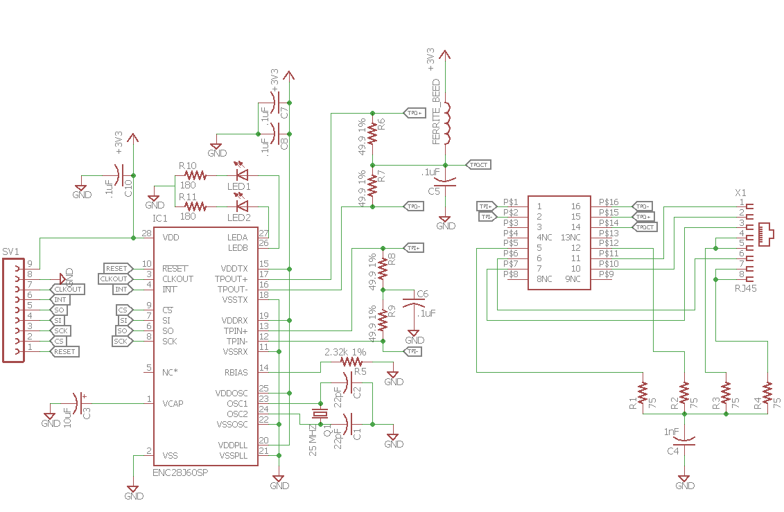
Design
Hardware
I made use of a broken network PC card and salvaged the RJ45 and pulse transformer (Bel S558-5999-46). This project could be made much smaller by using a RJ45 with built in transformer and LED’s (mag jack).
- The SPI clock (sck), chip select (CS), data in (SI), and data out (SO), are brought out to a header for easy connection. Additionally the clock output (outputs 6.25MHz at default), INT, RESET, 3.3v and GND pins will be useful to have on a header as well.
- The RESET, and CS pins have weak internal pulls ups and so don’t need external pull up resistors.
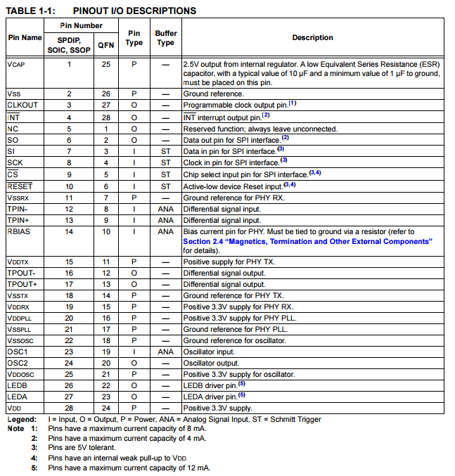
The ENC28j60 operates on 3.3v but its CS, SI, SCK and RESET pins are 5v tolerant, meaning the sending lines from MCU to ENC28J60 don’t need to be level shifted if the MCU is running on 5v. However a logic level converter may be needed for the receiving lines SO, INT and CLKOUT pins from ENC28J60.
- The ENC28J60 can operate in half duplex and full duplex modes (section 2.6 in data sheet). If LEDB’s current is sourced by LEDB pin the device will run in half duplex, otherwise if LEDB pin is sinking current, the ENC28J60 will auto configure itself for Full Duplex mode.
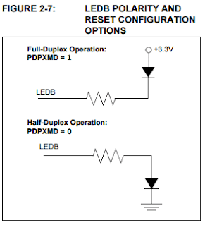
- Full duplex mode can transmit and receive at the same time without worry of packet collision - sounds great. However from section 9 in datasheet, the ENC28J60 does not auto-negotiate with the network controller to operate in full duplex mode. The ENC28J60 will be treated as a half duplex device, unless the network controller is manually configured to treat the ENC28J60 as a full duplex device. This doesn’t seem ideal so I chose the LED configuration such that the device will be configured for half duplex mode on startup. 10BaseT devices just weren’t meant to function as full duplex devices easily. Also this will probably be interfaced to 8-bit pic device in a later project and probably wont operate fast enough to take advantage of full duplex operation anyway.